IEEE EDS Workshop on VLSI Semiconductor Devices and Compact Modeling
Hosted by: IEEE EDS Student Branch Chapter
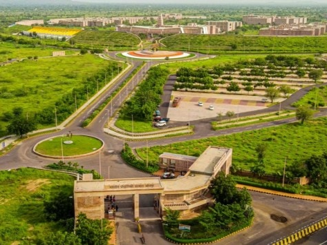
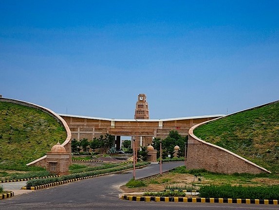
Indian Institute of Technology Jodhpur
21-24 December 2025
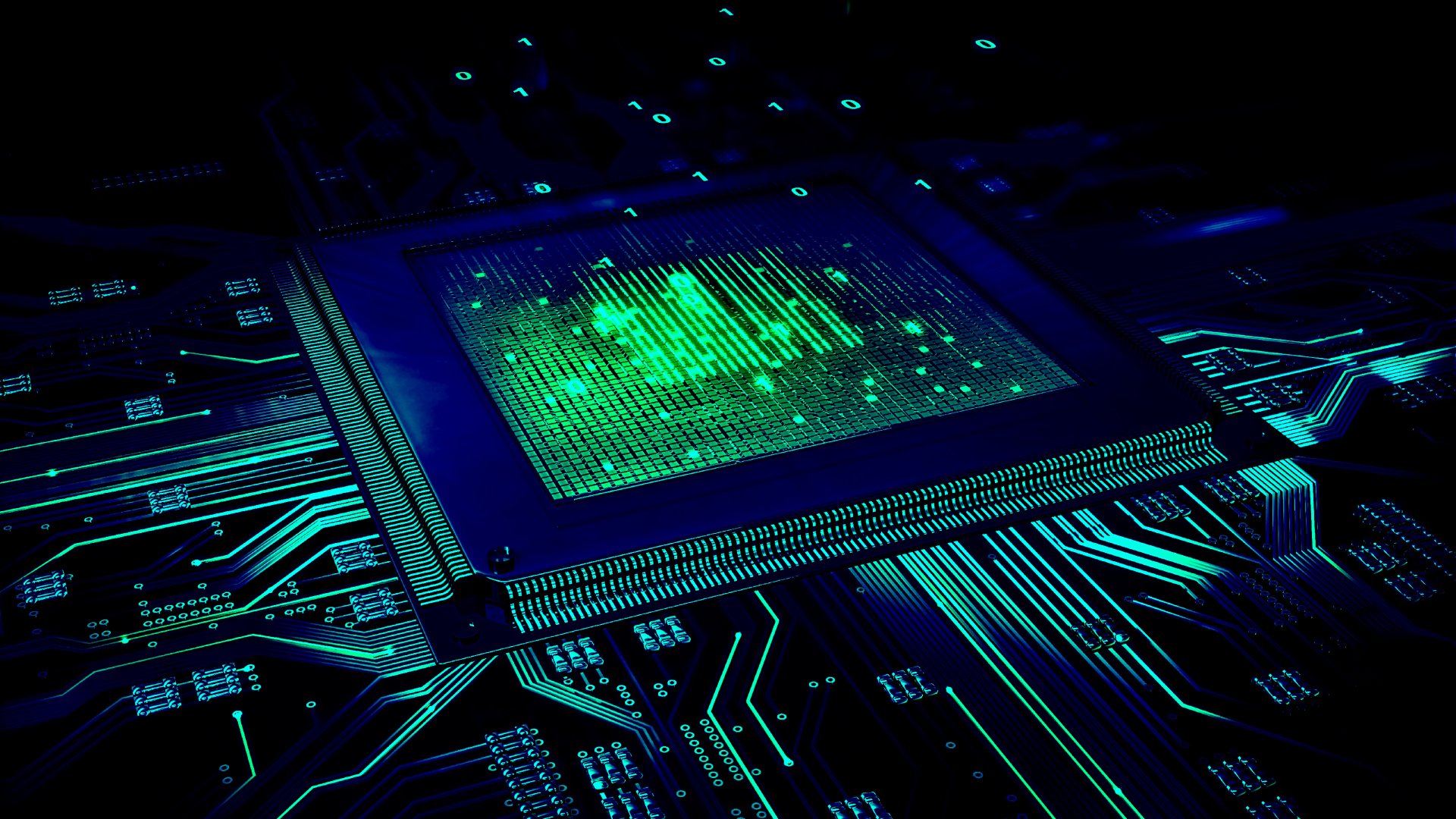
Bridging Physics and Simulation: The Future of Compact Modeling in VLSI
Explore how modern device physics and data-driven modeling converge to shape the next generation of semiconductor design and reliability.
About the Workshop
This IEEE EDS Workshop focuses on semiconductor device physics, compact modeling methodologies, and practical simulation workflows essential for advanced VLSI design. The sessions combine theoretical insights with hands-on training, covering emerging devices, reliability mechanisms, and ML-driven modeling approaches. Participants will gain a holistic understanding of how physics-based and data-driven models enable predictive, efficient design of future electronic systems.
When
Sunday to Wednesday
21-24 December 2025
Where
New LHB 103, Near Department of Electrical Engineering
IIT Jodhpur
What Will You Learn?
- Fundamentals of compact modeling and its role in modern VLSI design
- Advanced device concepts and their simulation using TCAD and SPICE frameworks
- Hands-on experience with TCAD, model calibration and parameter extraction
- Exposure to conventional and ML-assisted modeling workflows
Who Should Attend?
- Undergraduate and postgraduate students interested in semiconductor devices and circuits
- Research scholars and faculty focusing on device modeling
- Industry professionals working in design, TCAD, or compact model development
- Anyone keen to connect physical insight with practical modeling tools for circuit applications
Key Features
- Expert lectures by distinguished speakers
- Live demonstrations and guided tutorials on device and circuit simulation
- Live demonstrations of cutting-edge EDA tools
- Interactive discussions on modeling challenges in advanced technology nodes
- Networking opportunities and technical engagement with domain experts
Organizing Team
Prof. Harshit Agarwal
Chapter Advisor
Prof. Devendra Negi
Indian Institute of Technology Jodhpur
Prof. Pranay Ranjan
Indian Institute of Technology Jodhpur
Anant Singhal
Student Chair
Garima Gill
Student Vice-Chair
Yogendra Machhiwar
TreasurerTentative List of Speakers

Dr. Meyya Meyyappan
Ex-NASA Ames Research Center, USA
Dr. Andreas Kerber
Intel Corporation, Santa Clara, USA
Prof. Jong-Ho Bae
Yonsei University, Korea
Prof. Lan Wei
University of Waterloo, Cananda
Prof. Manoj Gupta
Indian Institute of Technology Jodhpur
Prof. Harshit Agarwal
Indian Institute of Technology Jodhpur
Prof. Devendra Negi
Indian Institute of Technology Jodhpur
Prof. Pranay Ranjan
Indian Institute of Technology Jodhpur
Dr. Pragya Kushwaha
Indian Institute of Technology JodhpurEvent Schedule
Registration
Kits and ID collection
Inauguration Ceremony
Welcome Address
Prof. Harshit Agarwal IIT Jodhpur
Introduction to Compact Modeling
Student Activities
Quiz and High Tea
Dr. Pragya Kushwaha IIT Jodhpur
How Chips Shape Nations and Careers
Lunch
Mess
Hands-on Session
EDA Tools for Device Design - Hands-on TCAD
Dr. Meyya Meyyappan Ex-NASA Ames Research Center, USA
Printed and Flexible Electronics and Devices
Student Activities
Quiz and High Tea
Prof. Manoj Gupta IIT Jodhpur
Photonic Devices and Applications
Lunch
Mess
Hands-on Session
EDA/ML Tools for Device Modeling and Simulation
Prof. Lan Wei University of Waterloo, Canada
Compact Models for GaN Devices
Prof. Pranay Ranjan IIT Jodhpur
Borophene: A New Sensation in Flatland
Prof. Devendra Negi IIT Jodhpur
Probing Atomic-Scale Magnetism via Energy-Filtered Differential Phase Contrast STEM
Excursion
Campus Tour and Lab Visit
Lunch
Mess
Hands-on Session
Fabrication of 2D-Material-based Devices
Dr. Andreas Kerber Intel Corporation, USA
Reliability of Metal Gate/High-K CMOS Devices
Valedictory Ceremony
Certificate Distribution
Event Venue
New LHB 103, Near Department of Electrical Engineering
Indian Institute of Technology Jodhpur
NH 62, Surpura Bypass Rd, Karwar
Jheepasani, Rajasthan - 342030, India
Sponsors
Registration
Registration is closed
For more info: nanodevicesandapplab@gmail.com
Contact
Address
Nano devices and Application Lab
Department of Electrical Engineering
Call Us
+91 8630 1177 09
Email Us
nanodevicesandapplab@gmail.com